

ARMv7 CPU Project
Overview
This project documents the development of a simplified ARM-inspired CPU written in Verilog. The implementation includes instruction decoding, ALU operations, branching, memory controllers, pipelining, hazard control, and a custom assembler.
The project was developed incrementally using extensive simulation, FPGA testing, and Verilog testbenches. The entries below document the development process chronologically.
Please refer to the Lab Spec.
Features
- Instruction decoder
- Arithmetic and logical ALU operations
- CMP and conditional branching
- Memory and data bus controllers
- Register array and program counter logic
- Instruction fetch and instruction cache
- Three-stage pipelining
- Hazard control
- Python assembler
7/24/2025 // Day0
Official project start day. I tried making some components in Verilog and used testbenches to simulate them yesterday. Things seemed doable.
Today I asked my Professor if I could use Verilog for the final project since we were supposed to only create this project in simulation software and, not on real FPGA fabric. However, permission was granted. Let's see how this ends up.
7/25/2025 // Setting Things Up
Project setup day.
First day of the project.
Part of the CMP component was completed with working Z and N flags. I was too tired to work with the C flag today, mainly because I was too tired to understand the logic behind it.
Assets

7/26/2025 // The World of CMP Instructions
Started the day by understanding CMP flags. Took me a while to go over everything regarding 2's complement to understand the C flag.
Completed the CMP component today. The flags are set at posedge clk to be used by the following branch instruction(s).
Assets

References
-
- Notes covering Verilog syntax and fundamentals.
-
"ARM Assembly: Lesson 7 (CMP)" by LaurieWired
- Very helpful in understanding how CMP works.
7/27/2025 // MemoryControl and DataBusControl
Starting out with MemoryControl today. Exntensive research was done on the working on MemoryControllers and inout ports. Perspective matters in this part of the project to understand flow of data. The required MemoryController was implemented in verilog. However, the testing was not as simple and produced invalid results.
After some research, I found out that to the inout ports need a wire to connect them since we would need to mimic the real-world implementation.
So I added a reg db_driver to have the testbench working.
The DataBusController was quite similar in implementation to the MemoryController, and thus was finished fairly quickly.
Assets


DataBusController Netlist View
References
- "How to write Verilog Testbench for bidirectional/inout ports"
- Helpful reference for understanding
inouttestbenches.
- Helpful reference for understanding
7/27/2025 // RegArray and Final Touches
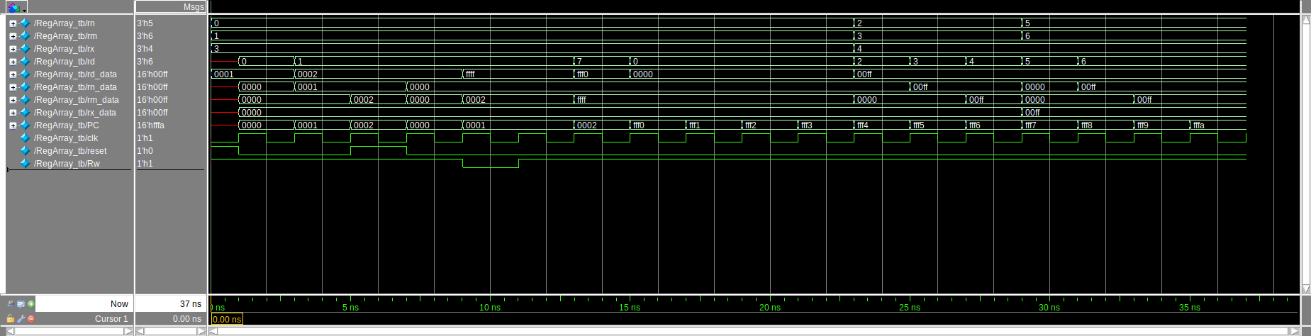
I added the following ports to the previous simple RegArray:
RxRx_dataRwPC
It was quite simple, but now I have a lot more to work with.
Assets

08/01/2025 // Instruction Decoding
Starting out with the instruction decoder today. Going through the ISA and lab spec, I used the instruction groups and morphed them into equivalent case and casez blocks. I laid out a structure to be used as a basis for ALU operations and other control signals.
I am now skeptical about a few things. The lab spec only gives me Imm11 for unconditional branches, which is not enough to traverse the 16-bit wide memory.
The official ARM docs mention it being sign-extended. I will consult with the Professor about this.
Assets
08/03/2025 // Assembling the ALU
Since AU and LU were supposed to be different units, I considered a signal called useAU to feed into the ALU. Considering the complexity of the ISA, this seemed like a simple working mechanism.
Turns out I don't actually need the useImm signal if I am already sending out ALU operations. That is very much by the design of the AU and LU. I also started assembling the top-level unit and attached the RegArray, ALU, and InstructionDecoder.
Although the ALU doesn't need useImm, I still need it for other components such as the CMP unit.
Assets
08/04/2025 // Make it make sense
This part of the project was made by oversimplifying everything, and then later refactoring to remove redundancy. The top-level CPU entity was put together along with some hex decoders to show register values on the fpga. I also made some videos along the way. Putting in the controllers was a bit tricky since there was no memory module involved at this stage. Testbenches were written to check for expected behaviour of the underlying modules.
Fortunately, the ISA had many unassigned opcodes, and a new MOV Rm -> Rd operation was added in the ALU.
Almost got the register/immediate arithmetic working and wrote testbenches for the same. The following video shows the CPU adding 1 to one of its register with CLK set to a button for testing. The value is read using hex decoders, and the CPU is reset at the end.
Assets
Adding Controllers to Top Level
08/05/2025 // Testing testing and testing
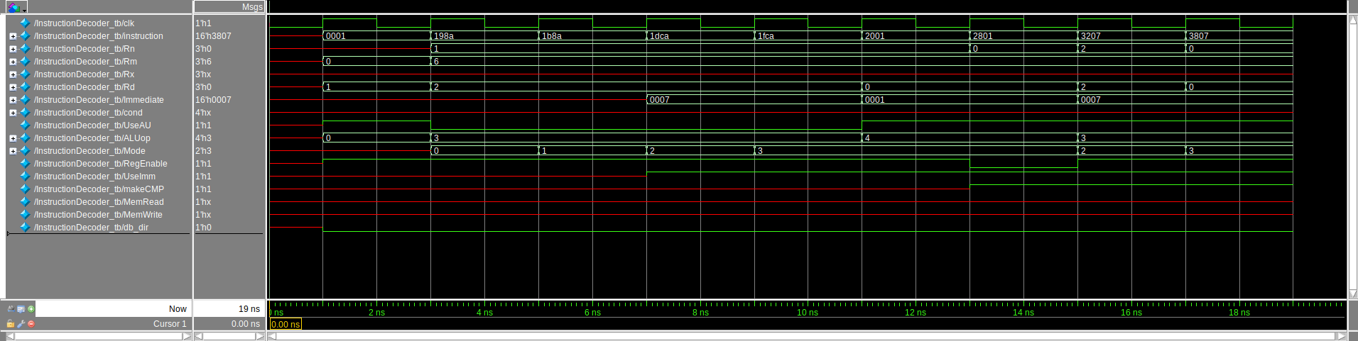
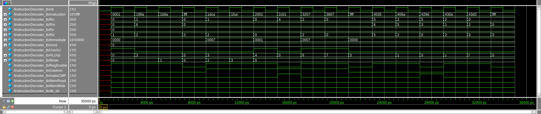
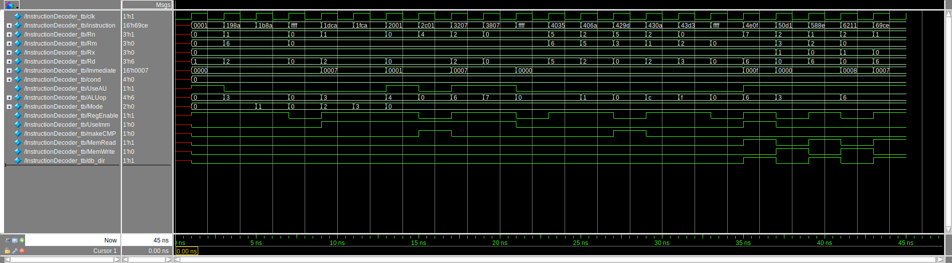
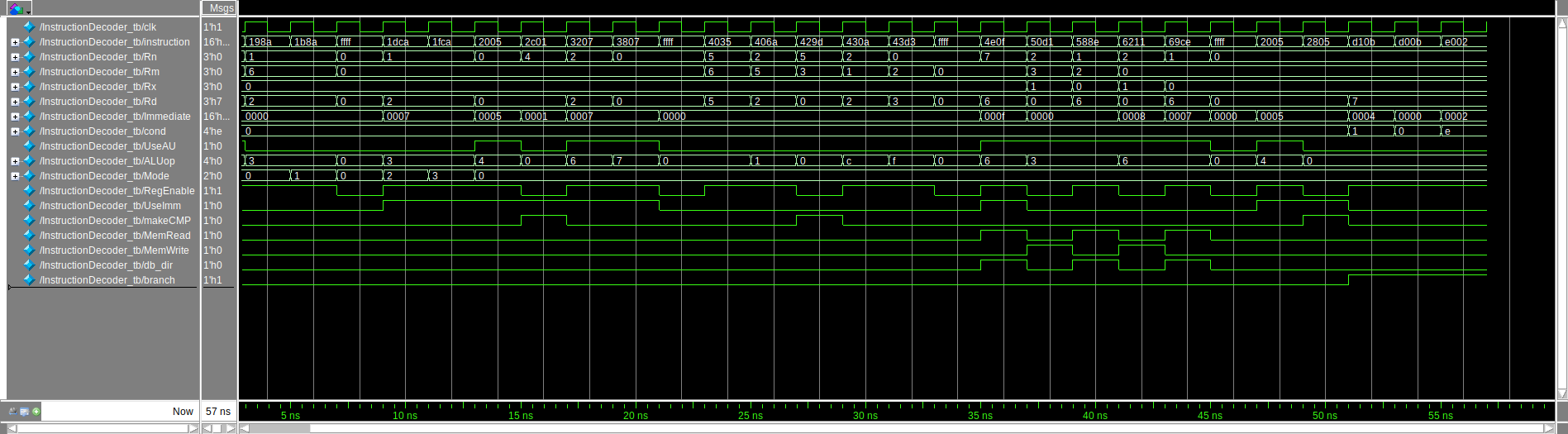
I plan on getting all the tests done and working for the InstructionDecoder today. The testing for logical operations pretty straightforward.
Moving on to the memory instructions, I was not sure if I needed a separate address calculation unit. I decided on re-using the ALU for this.
The ALU was given the required operation codes and aluOut was connected into the address line.
The memory management was a little tedious, but the data controllers from earlier were quite useful in manipulating the data and addresses. I eventually got the expected behaviour, at least on the testbenches.
Assets
Instruction Decoder Testbench Source
08/06/2025 // The Core of Control Flow
Today was the day for implementing branching. Although it is quite straightforward, there is some inconsistent behaviour with the current modules. According to Lab-4, everything in the RegArray should halt when Rw is low. However, there are many instructions where Rw needs to be low. For example, the CMP instruction has no intention of writing anything back to the register array. To avoid unwanted register changes, it is instinctual to simply set Rw low, but that would also freeze PC/r7.
For the moment, I am going to implement r7 so that it ignores Rw. I completed the branch instruction decoding, and with that, the instruction decoder is complete. I also added a branch module in the ARM assembly which writes to the program counter. If the branch condition is met, it writes the new branch address. Otherwise, it writes PC + 1.
The above was discussed and resolved with Professor. Discussion
Assets
08/06/2025 // It actually works!
I added an InstructionFetch unit and a simple InstructionCache using case statements before going to sleep.
It simply adds 2 to reg0, then branches back to repeat the same instruction. And it actually works. It's alive.
Assets
ARM Assembly Netlist with Instruction Fetch
08/08/2025 // Bits Assemble!
With working hardware comes working software. I will be starting my research into making assemblers today.
References
08/09/2025 // Assembling the Assembler
Going through the lab spec and lecture notes, the assembler required is fairly straightforward.
I started with writing some pseudocode.
The basic idea is to have a multi-pass approach:
- Remove comments and blank lines
- Calculate program counter addresses
- Create a symbols dictionary
- Expand any
BLinstructions using calculated symbols - Convert the final assembly into binary files
08/10/2025 // Assembling the Assembler - II
It was a bit tedious to implement the assembler.
I discussed the implementation details in the attached README.md, but I got it working.
Assets
References
08/13/2025 // Final Boss: Pipelining
I aim to finish pipelining the CPU today. Let's see how it goes.
To begin with, I started with some minor top-level refactoring.
The code looks way cleaner now.
I implemented two intermediate registers:
instruction[fromIF/toID]controlWord[fromID/toEX]
These registers are clocked, so the whole design is now divided into three stages:
- IF
- ID
- EX
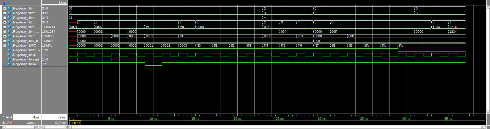
Next, it would be ideal to begin with stalling for branches. I had to fix some flaws in the RegArray. It did not increment the program counter when Rw was low. This followed the original lab specification, however, instructions with no writeback such as CMP would go into a loop because the PC would never increment.
Next, I needed to gatekeep the PC value irrespective of Rw in order to implement stalling. A simple PC_w signal does the job. I wrote some extra testbench steps and it works perfectly. I also had to include reset and flush signals for hazard control and startup.
Additionally, I had to do some research on what exact approach to take for stalling during branching. I will now need to implement a hazard control unit to manipulate these signals. It was fairly straightforward, but rather tedious. Part of the reason is probably me not discussing the specification in enough detail beforehand. Anyways, once register value stalling is implemented, this project should be ready.
Assets
Top Level Netlist (Pipeline Scaffolding)

References
08/14/2025 05:37 // Insert End Credits
The pipeline is developed. Hazard control is working. I have attached the top-level netlist with all the modules.
Assets
Final Thoughts
This project started as an attempt to explore Verilog and gradually evolved into a functional ARM-inspired CPU architecture with branching, instruction decoding, pipelining, hazard control, and a custom assembler.
The biggest lessons from this project were not necessarily tied to Verilog syntax, but rather:
- Thinking in terms of hardware data flow
- Understanding sequential versus combinational logic
- Debugging through testbenches
- Managing control signals across modules
- Handling architectural edge cases
- Understanding why pipelining complicates everything humans touch
Building the assembler also gave me a much better understanding of instruction set architecture design and how software interfaces with hardware at a lower level.
In the end, the project became far more than a course assignment.